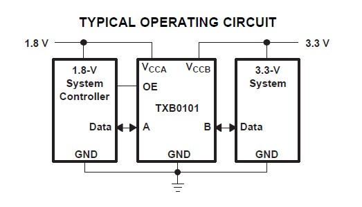
Product Summary
The TXB0101DBVR is fully specified for partial-power-down applications using Ioff. The Ioff circuitry of the TXB0101DBVR disables the outputs, preventing damaging current backflow through the device when it is powered down. To ensure the high-impedance state during power up or power down, OE should be tied to GND through a pulldown resistor; the minimum value of the resistor of the TXB0101DBVR is determined by the current-sourcing capability of the driver. NanoFree-package technology is a major breakthrough in IC packaging concepts, using the die as the package.
Parametrics
TXB0101DBVR absolute maximum ratings: (1)VCCA Supply voltage range –0.5 to 4.6V; (2)VCCB Supply voltage range –0.5 to 6.5V; (3)VI Input voltage range –0.5 to 6.5 V; (4)VO Voltage range applied to any output in the high-impedance or power-off state –0.5 to 6.5 V; (5)IIK Input clamp current VI < 0 –50 mA; (6)IOK Output clamp current VO < 0 –50 mA; (7)IO Continuous output current ±50 mA; (8)Tstg Storage temperature range –65 150 ℃.
Features
TXB0101DBVR features: (1)Available in the Texas Instruments NanoFree TM Package; (2)1.2 V to 3.6 V on A Port and 1.65 V to 5.5 V on B Port; (3)VCC Isolation Feature – If Either VCC Input Is at GND, All Outputs Are in the High-Impedance State; (4)OE Input Circuit Referenced to VCCA; (5)Low Power Consumption, 5-mA Max Icc; (6)Ioff Supports Partial-Power-Down Mode Operation; (7)Latch-Up Performance Exceeds 100 mA Per JESD 78, Class II.
Diagrams

| Image | Part No | Mfg | Description |  |
Pricing (USD) |
Quantity | ||||||||||||
|---|---|---|---|---|---|---|---|---|---|---|---|---|---|---|---|---|---|---|
 |
 TXB0101DBVR |
 Texas Instruments |
 Translation - Voltage Levels 1B Bidir Vltg-Level Translator |
 Data Sheet |

|
|
||||||||||||
 |
 TXB0101DBVRG4 |
 Texas Instruments |
 Translation - Voltage Levels 1B Bidir Vltg-Level Translator |
 Data Sheet |

|
|
||||||||||||
 (China (Mainland))


